The device was created in my spare time during the COVID‑19 period. You know those moments when you sit at your computer, lose track of time, and your mind starts wandering? That happened to me too. Eventually my thoughts landed on a simple question: How clean are PCBs coming from an EMS after assembly? (And if you think that’s a strange question — well, I’m the kind of person who gets curious about electronics, not cheese production.)
In my work, long‑term and flawless PCBA operation is a major concern — especially when failures appear without a clear explanation, such as issues caused by contamination or humidity. One part of this challenge is understanding how clean a PCBA really is when it comes straight from the factory.
A “real expert” might simply define an upper limit for PCB surface conductivity in mS/in² (or µS/cm²) and call it a day. But in practice, measuring this value is not that simple. There are specialized machines that can do it — you submerge part of the PCBA, or the entire board, in ultra‑pure water and measure the conductivity of the fluid.
This leads to the real question I wanted to solve: how can you measure extremely high resistance values without relying on expensive equipment?
Means to measure current
The first method is straightforward: measure the voltage drop across a shunt resistor. Since the voltage drop across a known resistor is proportional to the current, Ohm’s law allows you to calculate the resistance of the circuit.
The second method is to measure the magnetic field generated by current flowing through a conductor, using a Hall‑effect sensor or a current transducer. For Hall‑effect devices, Allegro offers excellent compact sensors such as the ACS750. For current transducers, companies like LEM provide reliable solutions.
Today’s microcontrollers are inexpensive and highly accurate, which means we can measure time very precisely. If the measured time correlates with current — for example, by observing how long it takes to charge a capacitor — we can also determine the resistance of the circuit. There are many demonstrations of this technique using discrete components, and they illustrate the concept well.
The last method I’ll mention is the transimpedance approach (TIA). It is similar to the shunt method, but instead of measuring the voltage drop across a physical resistor, the “resistor” is an operational amplifier configured as a current‑to‑voltage converter. In practice, this behaves like measuring across a resistor that is effectively approaching 0.00…0 Ω.
So naturally, I decided to start with the most exotic method.
The TIA approach appeals to me because it is complex, challenging, and time‑consuming — in the best possible way. Another reason I chose it is that it eliminates the need for a high‑voltage source. Measuring something like 1 GΩ often requires applying several kilovolts, which is dangerous and can easily cause arcing between PCB traces. In my application, I don’t need the exact resistance value; I only need to verify that the circuit can withstand a specific test voltage. High‑voltage methods are great for underground power cables, but not for delicate PCB assemblies.
In my design, the test voltage is only ±2.5 V, which is perfectly safe — but it also makes the measurement extremely sensitive to external noise and EOS/ESD effects. Remember, we are trying to detect signals in the picovolt range. Yes, picovolts.
What to build
When researching possible solutions, I found many interesting high‑end circuits online — some of them brilliant, but many relying on components that are practically unobtainable. My first choice was the ADA4530‑1 from Analog Devices, but COVID‑era shortages made it impossible to buy. Even today, availability is limited and the price is far too high for a DIY project (around 25 USD per chip).
A more realistic option came from Texas Instruments: the LMP7721. It costs roughly one‑quarter of the ADA4530‑1 and is actually available.
Datasheets for these components are a goldmine of knowledge. The op‑amp I selected includes excellent explanations and application notes, which significantly reduced the design effort. Of course, the lower‑cost part has its drawbacks — for example, it lacks the built‑in guard‑drive circuitry found in the ADA4530‑1. This means the guard signal must be generated using an external op‑amp. (The guard signal is a special potential used to block noise from external sources.)
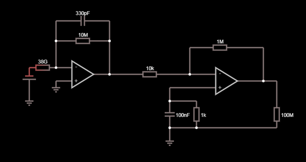
10M resistor that is above first from left op amp is input for my application ( in real schematic there is jumper so you can switch it from 10MΩ to 1GΩ – it suppose to give you 2 scales one form +/- 30pA and second +/- 3nA ).
Values that are on simulation diagram and voltage source for input 1 AA battery (1,55V) current that flow at input is 40,7pA – this value is translated to 40,7mV at the end – my DMM can easily read this value up to 3 decimal places so its good for me.
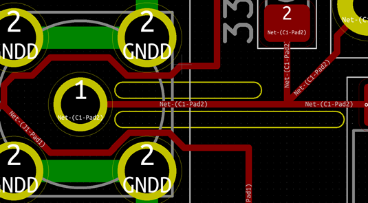
Key component in this simulation is precision for resistor and capacitor in this stage. Also that is not obvious – mechanical board for this device. Input stage have to be isolated from rest of PCB by slots / milled cuts around op amp input. Those yellow ovals around trace.
Last but not least — the wires used to connect the test samples. The LMP datasheet notes that for very low‑current applications, a special triaxial cable should be used. This type of cable consists of an inner signal conductor, a surrounding guard conductor, and an outer grounded shield. Unfortunately, triaxial cable is expensive, and the connectors are also costly and difficult to source. Roughly speaking, one meter of this cable can cost around 150 USD — definitely not ideal for an average DIY project.
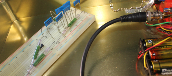
Verification circuit
Real life measurements started from checking circuit, cleaning PCB fev time in IPA and ultrasonic bath. Next – noise of system by it self(PCB was closed in reused metal cookie box with one hole for BNC output cable). For “standard reference” I chose few high resistant components from ROHM (1GΩ).

Small table was created in Excell and input of device was closed by end cap for SMA connector. Power up and 5 min of gathering data (my DMM have math functions like min max and avg). As you can see we have small offset (5,9mV) from beginning but we can resolve this issue later. DMM was set in DC range.
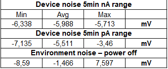
Last position in table can be explained by standing up from desk during measurement. Theoretically device is shielded from environment but DMM is grounded so some electrostatic field was created and detected.
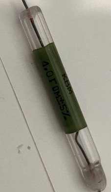
So next step – checking by “standards” 3x brand new 1GΩ 1% and one 10GΩ 2% from old soviet union (1980?). Values are display below.

Resistors from 1 to 3 supplied by one AA that have 1,5539V – so there is deviation form theoretical 1,5539nA to little bit hig – 1,57nA it mean ~1,22% off. For first run it great result. For vintage 10GΩ result was not so great from expected 153,9pA my DMM read 183,86pA. Desition was to not take to account this value because component is old and I cant confirm its true value.
After adjustment of output offset second measurement for the same sample was perform. Values are in table below. As you can see there are very close to expected simulated values. Deviation from calculated values is ~0,63%
In the end some useful links and key words that is nice to google like .:
SIR – surface resistance RV – volume resistance
https://www.circuitinsight.com/pdf/understanding_sir_ipc.pdf